Champs 20N1 Series Active Clamp Forward Solutions LT3753


20N1


20N1 Series LT3753 Based ACF Catalog

  • Footprint: 17.8 x 21.0 mm
  • Low Profile: 7.0mm Height
  • Proven in actual DC-DC converter using LT3753 IC.
  • Designs Available as Demonstration Boards.
  • Optimized for Opto Isolated Active Clamp Forward & Synchronous Rectifier Converter Design
  • Typical Efficiency 94%
  • Aggressive Interleave planar construction -- lowest achievable Leakage Inductance.
  • Multilayer PCB optimization for lowest AC resistance & Proximity Loss Effect.
  • Wide variety of PNs, Designs and Turns Ratios in stock. If not listed, Contact Us.
  • Integer Turns 1 thru 16 Available [Contact Us if Not Shown in Table].
  • Surface Mount, Thru-Hole, Pad-to-Pad, Embedded Planar Windings as Options

General Notes:

1.  This subset of Champs’ 20N1 series is earmarked to function in Opto Isolated Active Clamp Forward circuits as described by the LT3753 IC from Analog Devices.

2.  In other applications the 20N1 Series can operate over a wider Vin range or configured for different Input & Output Voltage and Rated Power. Increased height allows increased power output due to higher current capability.

3.  The Secondary Side SR FETs typically controlled by LT8311 Secondary Side IC. Direct Drive through Secondary winding ideal for Vin range 2:1

4.  Integer Turns available from 1T to 16T. Can be used as Primary or Secondary. Mechanical configuration and outline allow for a “flex” arrangement. Contact factory for information on any power topology design.

5.  All designs can be supplied with planar windings embedded in the pcb of the Main Module of the converter. Heat Sink and installed power components SM assembly and installation and incorporation into a module are also available.

1. Input Voltage Range 36-72.

Champs PN

Vin (Min)

Vin (Max)

Vout

Iout (Adc)

Pout (Watts)

Freq (KHz)

Volt-uSec [Rated]

Output Inductor PN

20N1-1202-80R

36

72

3.3

18.0

60

240

100

PQL2050-3R3-22-TH

20N1-0802-80R

36

72

5.0

12.0

60

240

100

20N1-1005

36

72

12.0

5.0

60

240

130

PQI2050-20HX-TH-10m

20N1-1012

36

60

24.0

2.55

60

240

130

PQI2050-100-6-LTC

2. Input Voltage Range 18-36.

Champs PN

Vin (Min)

Vin (Max)

Vout

Iout (Adc)

Pout (Watts)

Freq (KHz)

Volt-uSec [Rated]

Output Inductor PN

20N1-0702-40R

18

36

3.3

18.0

60

240

90

PQL2050-3R3-22-TH

20N1-0603-40R

18

36

5.0

12.0

60

240

80

PQL2050-4R9-14-TH

20N1-0606-40R

18

36

12.0

5.0

60

240

80

PQI2050-20HX-TH-10m

20N1-0612-40R

18

36

24.0

2.5

60

240

80

PQI2050-100-6-LTC

3. Input Voltage Range 9-18.

Champs PN

Vin (Min)

Vin (Max)

Vout

Iout (Adc)

Pout (Watts)

Freq (KHz)

Volt-uSec [Rated]

Output Inductor PN

20N1-0302

9

18

3.3

18.0

60

240

40

PQL2050-3R3-22-TH

20N1-0303

9

18

5.0

12.0

60

240

40

PQL2050-4R9-14-TH

20N1-0306

9

18

12.0

5.0

60

240

40

PQI2050-20HX-TH-10m

20N1-0312

9

18

24.0

2.5

60

240

40

PQI2050-100-6-LTC

LT3753 Product Page & DC2050A Ref Design:

https://www.analog.com/en/design-center/evaluation-hardware-and-software/evaluation-boards-kits/dc2050a.html#eb-overview

https://www.analog.com/en/products/lt3753.html

DC2050A

20N1 Series LT3753 Schematic -- [Optional LT8311 Secondary Side IC]

Schematic

20N1 Series LT3753 SR FET Secondary Winding Schematic

SM
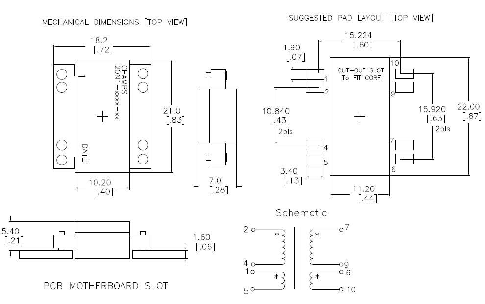
Mechanical Design Drawing 20N1 Surface Mount
Pad
Mechanical Design Drawing 20N1 Pad-to-Pad
PQL2050
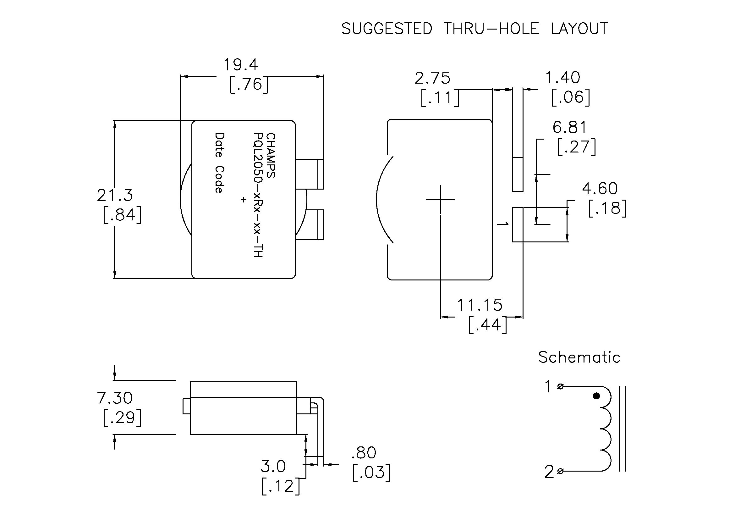
Mechanical Design Drawing PQL2050-TH Output Inductor